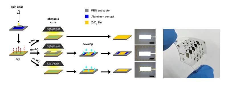
Photonic curing of solution-deposited ZrO2 dielectric on PEN: a path towards high-throughput processing of oxide electronics

Processing techniques that can achieve high-quality thin films while being compatible with high web speeds & high throughput are important for progress in thin film electronics. Application areas such as flat panel displays and photovoltaics use thin film electronic structures extensively, while adding process compatibility with flexible plastic substrates would enhance emerging applications like wearable sensors and biomedical devices. However, high-quality oxide films from solution-based precursors typically require 20 min or more of thermal annealing at high temperature (>250 °C) for each layer, severely limiting both the throughput and substrate choice. Here, we report high-speed photonic curing of ZrO2 dielectric thin films on flexible plastic substrates. The curing and patterning processes can be achieved simultaneously by using shadow mask patterning or adjusting conditions to convert oxide only on top of underlying metal contacts, i.e. self-aligned patterning. Metal–insulator–metal capacitors using two layers of ZrO2 films photonically cured in just 100 s per layer show non-dispersive capacitance–frequency behaviour from 102 to 106 Hz, high areal capacitance of 200 nF/cm2 and low dissipation factor of 0.03 at 105 Hz, leakage current density of ~10−7 A/cm2 at an applied field of 2 MV/cm, and a breakdown field of nearly 8 MV/cm. Using an upgraded tool, similar dielectric properties are achieved in as short as 100 ms using a single pulse of light, revealing a pathway to oxide film processing beyond 30 m/min.
Publications
Meet The Researchers

Name: Julia Hsu
Institution: University of Texas at Dallas