
Photonic curing of copper ink films on liquid crystal polymer substrate
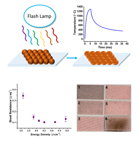
A recent increasing demand for flexible printed structures, for devices such as antenna arrays and frequency selective surfaces, has driven development of new processes. Researchers at UMass Lowell have developed techniques exposing intense pulsed light (IPL) to printed copper nanoparticle (CuNP) films which enables rapid curing on low-temperature substrates in ambient conditions. CuNP ink was printed using an aerosol jet technique on liquid crystal polymer (LCP; Vectra A resin), and was then cured using a high energy density light pulse. High-resolution SEM images of the cured films revealed that the CuNPs on LCP were fused together. Optimal curing parameters were a 5 ms pulse, 75% duty cycle, and an energy density range of 4.2–5.2 J·cm-2. Sheet resistance, Rs, values as low as ~0.1 Ω·sq-1were obtained. The LCP substrate took on a yellowed appearance after the application of five pulses and exhibited a surface free energy increase. A filter that blocked wavelengths <450 nm was placed over the printed copper film on LCP. As expected, the presence of the filter decreased the total energy density and produced a cured film with high Rs; however, when the energy density was increased in the presence of the filter, the Rs remained high (0.95 Ω sq-1).
Publications
Meet The Researchers

Name: Guinevere Strack
Institution: University of Massachusetts Lowell

Name: Alkim Akyurtlu
Institution: University of Massachusetts Lowell